Removal of Intellectual Property From Multi-Project Wafers
Removal of Intellectual Property Process
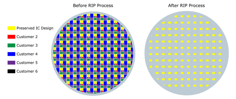
Some Integrated Circuit foundries can place several designs from multiple customers on one wafer called a Multi-Project Wafer, or MPW. This sharing of wafer masks saves customers money because IC fabrication costs are very high. Foundries also use the term "shuttle runs" in reference to MPWs.RIP, or Removal of Intellectual Property, is a laser process LSG developed to remove other customers' integrated circuit designs from an MPW while leaving specified IC designs intact. This allows standard wafer level testing to be performed instead of die level testing. In many cases, the entire RIP process can be completed within 48 hours.
LSG's Intellectual Property Removal process details:
- A custom program is created based on a project die map provided by the customer
- The location and measurements of all preserved die dimensions are confirmed
- A 200µm exclusion zone (EZ) is added around the protected area
- Accuracy can be maintained to within 10µm
- A custom schematic is created and sent to the customer for approval
- A trial run is performed to check the proximity of cuts to the die pieces
- A blanket coat of photoresist is applied for wafer protection
- A laser is used to process the wafer. Material is removed to a depth of 30-40µm
- A detailed inspection is performed
- The processed wafers are stripped of the photoresist layer and cleaned in a class 100 clean room environment
- The wafers are packaged and shipped