Trusted Wafer Coring Service
for Diverse Materials
wafer-coring_example
A 200 mm silicon wafer has been resized into two 100 mm wafers, each with several wafer flats. The primary wafer flats have been precisely matched to the notch of the original wafer.
Introduction
Wafer coring, also referred to as wafer resizing or downsizing, plays a pivotal role in semiconductor production. This method entails adjusting the diameter of a wafer to align with specific processing machinery. WaferFab Services specializes in coring various types of wafers, such as silicon, up to 12" (300 mm) in diameter, into smaller dimensions. We handle all standard wafer sizes, ranging from 2 inches to 12 inches. Our offerings are tailored to patterned and blank wafers, which can be tailored to any shape or size, be it circular, square, notched, or with multiple flats.
Why Wafer Resizing is Needed
As the semiconductor industry progresses, the growth in wafer sizes poses challenges for current process tooling made for smaller wafers. The immediate replacement of costly tooling may not always be practical. Resizing wafers to match existing equipment presents a budget-friendly option, enabling manufacturers to sustain use of their current tools as they strategize for future enhancements.
Upgrading equipment can cost millions, while resizing wafers is a fraction of that.
Mechanical Coring vs. Laser Cutting
WaferFab Services uses a mechanical coring process instead of lasers. This choice is driven by the variety of materials we handle, such as silicon, glass, sapphire, and composites. Mechanical cutting is versatile and does not depend on the material's ability to absorb laser energy. Our processing tools ensure precise cutting and edge beveling, making the process more cost-effective than laser cutting.
Materials We Process
Our mechanical coring process can handle a wide range of materials, including:
- Silicon
- Germanium
- Gallium Arsenide
- Silicon Carbide
- Glass
- Quartz
- Sapphire
- Ceramic Materials
We primarily focus on silicon wafer coring but are equipped to process any hard and brittle material. We can also handle multi-material stacks. (i.e. Silicon bonded to glass)
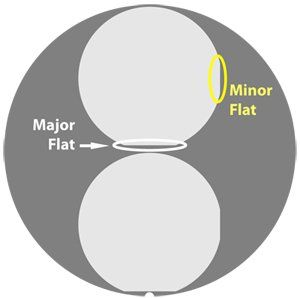
Flats and Notches
Flats and notches on silicon wafers serve two main purposes:
- They provide a reference surface for automatic handling equipment, ensuring precise alignment during lithographic processes.
- They indicate the wafer's crystal orientation, which is crucial for certain applications. Wafers smaller than 200 mm typically have flats, while those 200 mm and larger have notches to minimize real estate loss. Maintaining the orientation of flats and notches during resizing is essential, as is rounding or beveling the wafer edge after coring.
- The coring can be offset such that the original notch or flat is captured by the new wafer.
WaferFab's Standard Coring Process Workflow
- Protective Coating: To safeguard against surface damage, a protective layer, typically made of photoresist, is applied to the top of the wafer.
- Thickness Adjustment: Wafers are thinned as necessary to achieve the specified thickness.
- Customized Programming: A tailor-made program is developed in accordance with the customer's requirements.
- Cutting Process: Wafers are precisely cut to the desired dimensions and shape.
- Edge Beveling: When needed, the resized wafers are beveled at the edges to improve mechanical stability.
- Quality Inspection: A comprehensive inspection is conducted to ensure adherence to quality standards.
- Cleaning Procedure: The protective layer is removed, and the wafers are thoroughly cleaned.
- Packaging and Delivery: The processed wafers are packaged and sent back to the customer.
Conclusion
Wafer coring plays a crucial role in semiconductor manufacturing by allowing the utilization of current tooling while cutting down on expenses. WaferFab Services provides precise and cost-efficient mechanical coring for a variety of materials, guaranteeing top-notch results for all your wafer resizing requirements.